 |
"The conversion efficiency of solar cells has increased by a maximum of 10%". Toshiba Mitsubishi Electric's industrial system has developed an atomized CVD (chemical vapor deposition) device “TMmist†that forms a thin film by making raw materials into a mist. Since a non-vacuum process is used and no plasma is used, it is expected to reduce the installation area and initial investment of the device and improve the properties of the substrate film. The Toshiba Mitsubishi Electric Industrial System will target the use of solar cell transparent conductive films and will strive to obtain orders of approximately 1 billion yen in 2014 and approximately 2 billion yen in 2015.
Ultrasonic atomization
Existing sputtering apparatuses and the like using a vacuum process require auxiliary facilities such as a vacuum chamber and a vacuum pump. With the enlargement of the substrate, the installation area and initial investment of these devices will increase significantly. It is also impossible to avoid plasma damage to the substrate film.
Therefore, the Toshiba Mitsubishi Electric system aims to target film formation techniques using non-vacuum processes without plasma damage. The company looks at atomized CVD technology researched at Kyoto University in Japan, and based on this technology, it has been committed to productization since 2007.
The TMmist consists of (1) an ultrasonic atomizer for making a raw material into a mist, (2) an elongate rectifying nozzle for supplying mist-like raw material to a substrate with a width of about 1 m flowing on a production line, and (3) a heater for heating a substrate. figure 1).
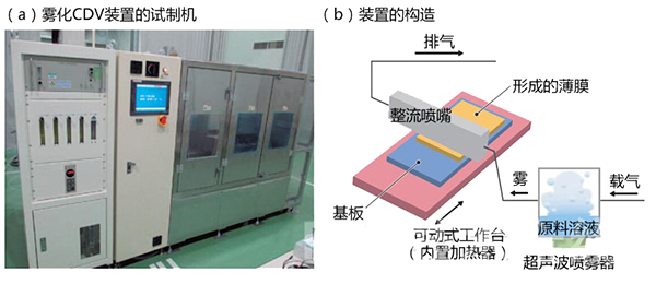
Figure 1: Atomization of raw materials using ultrasound
Toshiba's Mitsubishi Electric Industrial Systems developed an atomized CVD device (a). After the raw material solution is atomized by ultrasonic waves, the reaction is decomposed on the substrate to form a thin film (b).
The specific operation is as follows. Firstly, (1) Ultrasonic nebulizer was used to make the film-forming raw material solution into a mist-like droplet with a diameter of several μm using ultrasonic waves of 1.6M to 2.4 MHz. Next, the mist-like raw material is mixed with the carrier gas and sent to the (2) rectifying nozzle and sprayed onto the substrate. Then, the raw material (3) sprayed onto the substrate decomposes and reacts under the thermal effect of the heater to form a thin film.
The biggest issue in the realization of productization is how to optimize the thickness of the film and film quality has a significant impact on the problem of (2) rectification nozzle internal structure. At this time, it is necessary to use a rectifying nozzle to homogenize the atomized raw material and spray it onto the substrate. Toshiba Mitsubishi Electric Systems, with the assistance of its parent company Mitsubishi Electric, has repeatedly analyzed the relationship between the flow of atomized raw materials and the internal structure. In addition, the composition of the raw material solution used in (1) the ultrasonic atomizer was also optimized, and the mechanism of the (3) heater was also improved, thereby realizing the uniform heating of the large-area substrate.
Note 1) The amount of ultrasonic waves leaking to the outside of the device conforms to the standards of the I Semiconductor Equipment and Materials International.
Note 2) When forming a transparent conductive film on a substrate with a width of 1m, the film thickness unevenness is ±20%. By arranging a plurality of rectifying nozzles on the production line and repeating the film formation, the unevenness of the film thickness can be reduced to ±10%.
With the above measures, TMmist can obtain a film quality equivalent to a sputtering device. Taking the characteristics of a transparent conductive film as an example, the sheet resistance value reaches 9.5 Ω/□, and the average visible light transmittance at a wavelength of 400 to 800 nm reaches 90.5%. Note 3). It can meet the standard of 10Ω/□ or less and more than 80% required for the transparent conductive film of solar cells (Fig. 2).
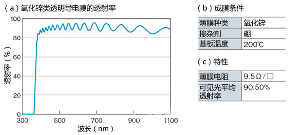
Figure 2: Average visible light transmission reaches 90.5%
The sheet resistance of the transparent conductive film formed by the atomization CVD method reached 9.5 Ω/□, and the average transmittance of visible light with a wavelength of 400 to 800 nm reached 90.5%.
Note 3) When forming a zinc oxide (ZnO) transparent conductive film, a raw material solution made of a zinc compound or the like is used. The substrate was heated to 200° C. with a heater, and ozone was supplied to the substrate to promote the reaction. The temperature unevenness on the substrate is ±2%.
no damage
This device is superior to the sputtering device in that it can not only reduce the large installation area and initial investment when using a non-vacuum process, but also improve the characteristics of the substrate film by virtue of the absence of plasma damage.
Among them, the good effect without plasma damage was confirmed by solar cell manufacturers. According to a manufacturer's report, when a transparent conductive film for a CIGS (Cu-In-Ga-Se) type solar cell is used, "the conversion efficiency (maximum) is improved by 10%." Encouraged by the good results, solar manufacturers have begun to consider importing prototype machines.
In addition, the deposition rate is higher than that of the sputtering apparatus. The sputter device was about 200 nm/min, while the TMmist reached 650 nm/min. The reason for this is estimated to be that the mist-like liquid can realize more raw material supply than the gas.
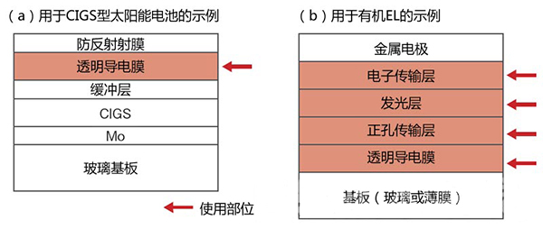
Figure 3: It can also be used for organic EL, etc.
Toshiba Mitsubishi Electric's industrial system envisages the use of an atomized CVD device for the use of transparent conductive films for CIGS solar cells, and it also considers the use of organic EL.
As the first application field of TMmist, Toshiba Mitsubishi Electric's industrial system selects the transparent conductive film of the CIGS solar cell that is expected to grow in the future. In the future, the company will also develop other applications such as transparent conductive films used in displays and organic EL materials using organic materials (Figure 3). Among them, in terms of organic EL, it can be used not only for a transparent conductive film but also for a light emitting layer, an electron transport layer, a positive hole transport layer, and the like. (Reporter: He Jiji, "Nikkei Electronics")
Eva Foam Puzzle is made from Eco-friendly, closed cell, non-smell and non-toxic Eva Foam material.
It consists of 9 pieces small puzzles, printed with beautiful and colorful pattern. You don't have to worry about it to be wet, cause the material is closed cell and antibacterial. Besides, when the puzzle is wet, it can just put on the wall, and won't fell, brining a lot fun for children and baby when in bathroom.

Eva Foam Puzzle,Foam Puzzle,Eva Foam Mat Puzzles,Eva Foam Animal Puzzle,Eva Foam Alphabet Puzzle ,Eva Foam Soft Puzzle
Huizhou Melors Plastic Products Factory , https://www.melorsfoam.com